Russian Startup Claims 3,000x Faster Electron Beam Lithography Amid Sanctions
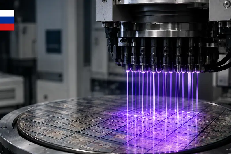
- A Russian startup proposes a multi-beam electron lithography system that could reduce wafer processing time by approximately 3,000 times compared to current electron beam methods.
- The innovation centers on a multi-cathode component with independent electron sources, simplifying complexity and cost compared to other multi-beam approaches.
- While the core multi-cathode element has been successfully tested, a complete working prototype of the lithography machine is still at least three years away from completion.
- This project is a direct response to Western sanctions imposed on Russia, compelling domestic efforts to develop indigenous semiconductor manufacturing capabilities.
In a bold move that could redefine its domestic semiconductor ambitions, a Russian startup, supported by the country's National Technology Initiative, has announced a revolutionary multi-beam electron lithography project. The team behind the initiative claims their technology could dramatically cut the time required to process silicon wafers from an astonishing one to two weeks down to just five to seven minutes, a reported 3,000-fold acceleration compared to existing electron beam lithography techniques. This development arrives as Russia grapples with stringent Western sanctions, forcing it to seek self-reliance in critical technological sectors like chip manufacturing.
Quick summary
- A Russian startup proposes a multi-beam electron lithography system that could reduce wafer processing time by approximately 3,000 times compared to current electron beam methods.
- The innovation centers on a multi-cathode component with independent electron sources, simplifying complexity and cost compared to other multi-beam approaches.
- While the core multi-cathode element has been successfully tested, a complete working prototype of the lithography machine is still at least three years away from completion.
- This project is a direct response to Western sanctions imposed on Russia, compelling domestic efforts to develop indigenous semiconductor manufacturing capabilities.
Why it matters
This initiative carries significant implications for Russia's strategic independence in technology. Cut off from advanced Western chip-making equipment since 2022, Russia is under immense pressure to develop its own semiconductor ecosystem. A successful domestic lithography machine, even if not cutting-edge by global standards, could enable local production of chips essential for defense, infrastructure, and other critical sectors, mitigating the impact of sanctions. For the global semiconductor industry, it highlights the potential for alternative lithography methods to emerge, albeit with substantial developmental hurdles. It also underscores how geopolitical pressures can spur localized innovation, potentially leading to new technological pathways outside of established norms. However, the lengthy development timeline means that even if successful, the technology could face challenges in keeping pace with the rapid advancements of the global industry, impacting its commercial viability beyond domestic needs.
Background
Semiconductor manufacturing hinges on lithography, the most critical and complex step where intricate circuit patterns are etched onto silicon wafers. For decades, the industry has relied predominantly on optical lithography, with Dutch giant ASML holding a near-monopoly on advanced extreme ultraviolet (EUV) systems that define the smallest features in today's leading-edge chips. Electron beam lithography, while offering superior resolution by 'drawing' circuits directly with electron beams, has historically been too slow for mass production, relegated primarily to research and low-volume, specialized chip fabrication. The process is inherently sequential, with a single beam meticulously tracing each pattern, consuming days or even weeks for a single wafer.
The geopolitical landscape dramatically shifted for Russia following its actions in Ukraine in 2022, triggering a cascade of international sanctions. These restrictions severely curtailed Russia's access to advanced semiconductor technology, including crucial lithography equipment from companies like ASML. This isolation spurred a national imperative to cultivate indigenous capabilities, leading to projects like the one announced by Evgeny Givargizov's team. Previous efforts often involved attempting to reverse-engineer or replicate existing technologies, but this new approach signifies a pivot towards novel solutions, driven by necessity rather than market competition.
Qnews24h insight
The Russian startup's announcement of a 3,000-fold speed increase in electron beam lithography, while impressive on paper, must be viewed through a pragmatic lens. It represents a significant scientific achievement in component development, specifically the multi-cathode, which addresses a core bottleneck of traditional electron beam methods. However, the gulf between a validated component and a fully functional, industrially viable lithography machine is vast, requiring years of engineering, integration, and capital investment. The estimate of 'at least three years' for a prototype, as noted by independent expert Sergey Varnavsky, raises concerns about technological obsolescence. The global semiconductor industry advances at an unrelenting pace; what is innovative today might be a generation behind by the time it reaches commercial readiness. This project appears to be less about global market disruption and more about a strategic, domestically-focused effort to circumvent sanctions and secure critical national capabilities, even if the resulting technology operates at a slower pace than the world's most advanced fabs. Its ultimate success will be measured not by global competitiveness, but by its ability to provide Russia with a viable, albeit perhaps less efficient, path to semiconductor self-sufficiency.
The Multi-Cathode Breakthrough
The core of the Russian team's innovation lies in its novel approach to multi-beam electron lithography. Traditional electron beam systems rely on a single electron beam to sequentially 'draw' patterns onto a wafer, a process akin to writing with a single pen. The proposed solution, led by Evgeny Givargizov, employs a 'multi-cathode' design – essentially a single base containing numerous independent electron sources operating in parallel. This can be visualized as using thousands of pens simultaneously on the same piece of paper, dramatically accelerating the process by dividing the work across multiple emitters.
Unlike other multi-beam systems under development internationally, which typically start with a single electron beam and then split it into multiple sub-beams using complex optical and shielding systems, the Russian design creates multiple independent electron sources from the outset. This direct approach is said to significantly reduce the complexity, infrastructure requirements, and overall cost of the equipment. The team reports successfully developing and testing this multi-cathode component, achieving an impressively small tip radius of just 1.5 to 2 nanometers, a result described as among the best globally for this type of electron beam lithography.
Comparing Speeds: A Nuanced View
While the claim of being 3,000 times faster than existing electron beam technology is striking, it is crucial to understand the context. This acceleration is relative to older, single-beam electron lithography methods. When compared to the cutting-edge optical lithography machines produced by ASML, the picture changes considerably. ASML's advanced systems can process entire silicon wafers in mere seconds or tens of seconds, mass-producing chips at an industrial scale. The Russian startup's target of five to seven minutes per wafer, while a monumental improvement for electron beam, still trails far behind the throughput capabilities of ASML's optical lithography.
This distinction highlights that even with a breakthrough in electron beam speed, the technology may not be competitive for high-volume, leading-edge chip production on the global market. Instead, its primary value proposition for Russia could lie in enabling domestic production for specific applications where high resolution is paramount and mass-market speed is a secondary concern, or for foundational chips not requiring the absolute latest process nodes.
From Component to Commercial Reality: A Long Road Ahead
It is vital to reiterate that the announced achievement is the successful fabrication and testing of the multi-cathode component, which forms a critical part of the proposed machine. The complete electron beam lithography system itself does not yet exist and has not even entered the detailed engineering design phase. The research team projects a minimum of three years to develop the first operational prototype, contingent on sustained funding and smooth progression through the complex development stages.
Commercialization, if it ever materializes, would be a much longer journey after the prototype stage. As independent technical expert Sergey Varnavsky cautions, the rapid evolution of global semiconductor technology means that by the time a full prototype is ready in three years, the market may have moved on. Such a device could potentially be obsolete for international competition before it even launches. However, within Russia's domestic market, which is largely insulated from international competition due to sanctions, the equipment could still find willing users, addressing a critical supply gap.
This project, regardless of its ultimate commercial fate, serves as a testament to the powerful influence of geopolitical realities on technological development. Facing severe restrictions, Russia is compelled to forge its own path in high-tech manufacturing. The multi-cathode's successful testing indicates that this alternative scientific direction holds promise. The next three years will be a crucial litmus test, demonstrating whether scientific feasibility can be translated into a practical, industrial-scale machine capable of bolstering Russia's technological autonomy.

Image: AI-generated depiction of a chip manufacturing facility.

Image: Russian 350 nm lithography equipment.
Sources
Why it matters
This initiative carries significant implications for Russia's strategic independence in technology. Cut off from advanced Western chip-making equipment since 2022, Russia is under immense pressure to develop its own semiconductor ecosystem. A successful domestic lithography machine, even if not cutting-edge by global standards, could enable local production of chips essential for defense, infrastructure, and other critical sectors, mitigating the impact of sanctions. For the global semiconductor industry, it highlights the potential for alternative lithography methods to emerge, albeit with substantial developmental hurdles. It also underscores how geopolitical pressures can spur localized...
Background
Semiconductor manufacturing hinges on lithography, the most critical and complex step where intricate circuit patterns are etched onto silicon wafers. For decades, the industry has relied predominantly on optical lithography, with Dutch giant ASML holding a near-monopoly on advanced extreme ultraviolet (EUV) systems that define the smallest features in today's leading-edge chips. Electron beam lithography, while offering superior resolution by 'drawing' circuits directly with electron beams, has historically been too slow for mass production, relegated primarily to research and low-volume, specialized chip fabrication. The process is inherently sequential, with a single beam meticulously...
The Russian startup's announcement of a 3,000-fold speed increase in electron beam lithography, while impressive on paper, must be viewed through a pragmatic lens. It represents a significant scientific achievement in component development, specifically the multi-cathode, which addresses a core bottleneck of traditional electron beam methods. However, the gulf between a validated component and a fully functional, industrially viable lithography machine is vast, requiring years of engineering, integration, and capital investment. The estimate of 'at least three years' for a prototype, as noted by independent expert Sergey Varnavsky, raises concerns about technological obsolescence. The...
References
Editorial information
The editorial team reviews sources, adds context, and structures stories so readers can understand the news more clearly.
Article from QNEWS24H
Comments
(0)No comments yet. Be the first to share your thoughts.